Navigation : EXPO21XX > RENEWABLE ENERGY 21XX >
H29: Universities - Renewable Energy Research
> Australian National University - CECS
Australian National University - CECS

Videos
Loading the player ...
- Offer Profile
- Research into solar energy
technologies at CSES is aimed at increasing the uptake of environmentally
benign solutions by making solar energy cheaper and the conversion process
more efficient. Some of the research looks at new technologies and other
research looks at news ways to increase the efficiency of existing
technologies, much of this effort has lead to technology transfer to
commercial solar energy projects.
Product Portfolio
RESEARCH
Hybrid systems
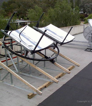
- In concentrator photovoltaic (CPV) systems, sunlight is focussed using optics such as mirrors and lenses to form a point or a line. The photovoltaic (PV) cells are placed at the focus of the optics where they receive concentrated light. These systems offer several advantages over flat plate photovoltaic systems, including the replacement of costly solar cells with inexpensive optics (hence reducing overall system costs). Due to the increased concentration of light onto the cells, cells must be either passively or actively cooled to ensure optimum performance. However, this heat introduces the option of creating a hybrid CPV-thermal (CPV-T) system which can generate both electrical and thermal energy from a single integrated system. At CSES a range of linear, single-axis tracking hybrid systems (and their components) are studied.
Microconcentrator
- The microconcentrator (MCT) system is a linear,
single-axis tracking CPV-T system being developed in partnership with
Chromasun Inc., based in the U.S.A.. The system operates at concentration
ratios of up to 30X.
Most CPV and CPV-T systems are significant structural installations. Hence, unlike conventional flat plate PV systems, they are generally unsuitable for domestic and commercial rooftop applications. The microconcentrator system reduces the size and weight of all components, resulting in a system which is suitable for rooftop installation. In addition, hybrid receivers allow the option of producing both electrical and thermal power from a single unit. The target performance of each box is to simultaneously produce 2 kW of thermal power and 500 Wp of electrical power.
One of the key design features of the MCT is the sealed enclosure. This enclosure is 3.0m long, 1.2m wide, and 0.3m deep and isolates all the functional components of the system from external environmental influences such as wind loading, humidity, and soiling. The removal of the effect of wind loading on the optics allows the use of a Fresnel array of ultra lightweight reflectors which require no structural support other than tensioning at mounting points at each end of the enclosure.
Spectral splitting
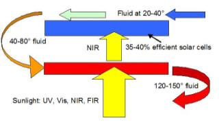
- A limitation of many conventional CPV-T systems is that
the desire to have the circulating fluid cool the cells conflicts with the
desire to achieve a high temperature fluid. CSES is now working with UNSW,
CSIRO, Chromasun, and NEP to develop a hybrid CPV-T system that can very
efficiently deliver both 150˚C heat and solar electricity. The key technical
goal of the project is to use spectral splitting to thermally decouple the
solar cells from the 150˚C circulating fluid.
Silicon solar cells waste most of the energy of the solar spectrum. When illuminated by the whole solar spectrum, silicon linear concentrator cells have a solar conversion efficiency of 20%. However, when illuminated by monochromatic light of wavelength around 1100nm, the conversion efficiency of a silicon concentrator cell approaches 50%.
The linear hybrid CPV-T receivers being developed will split sunlight into several bands based on wavelength. The near infrared light (700-1120nm) will be directed to PV cells. The cell efficiency when illuminated by this wavelength range is 35-40%. The balance of the solar power is converted to heat, and is used to pre-heat the thermal fluid. Since the conversion efficiency for this spectral range is high, the cells have substantially reduced cooling requirements. UV and visible light (<700nm) and FIR (far infrared) light (>1120nm) will be absorbed by a thermally insulated absorber. About two thirds of the solar power is in this wavelength range, allowing heating of the thermal fluid to 150 ˚C. Since the thermal and the PV absorbers are decoupled, the thermal fluid can reach high temperatures while the solar cells remain cool.
There are many possible spectral split options, utilizing selective absorption, reflection and refraction. The most promising configurations and designs are being selected based on a cost benefit analysis.
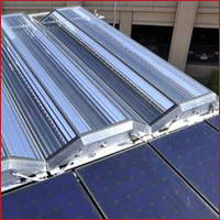
Combined heat and power solar (CHAPS) systems
- CSES, in collaboration with the Solar Thermal Group, have
developed large-scale, linear CPV-T systems based on parabolic trough
mirrors. Demonstration systems have been constructed at Rockingham in Perth
and at ANU’s Bruce Hall.
HIGH PERFORMANCE SILICON SOLAR CELLS DESIGNED FOR CONCENTRATION APPLICATIONS
High-performance silicon solar cells were designed and manufactured for systems operating in the range 10-60X. These cells operate at high efficiencies (20-24%) and can be obtained at moderate cost using an elegant process sequence. Cells are integrated into concentrator receivers which feature thermal cycling stress relief, bypass diodes, and encapsulation. The receiver can have either a light weight aluminium fin heatsink, or water cooling.
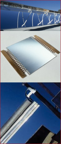
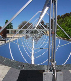
PARABOLIC TROUGH MIRRORS
Mirrors are constructed using an elegant glass-on-metal-laminate technology in which thin rear-silvered glass mirrors are bonded to a coated steel sheet. Stamped tab ribs are fitted to the end of the sheet to produce the correct parabolic profile. This construction produces a lightweight, durable mirror.
RECEIVERS ARE MOUNTED AT THE LINE FOCUS OF THE MIRRORS
Nanostructures for photovoltaics
- Nanotechnology is the science of the small. It involves using new scientific understanding and new fabrication techniques to achieve much greater control over the properties of materials and devices. Nanotechnology has the potential to allow solar cells to be more efficient and thinner, both of which would make solar cells cheaper. In this project we are focusing on nanophotonics, that is, using nanotechnology to improve the optical properties of solar cells.
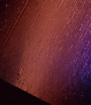
Nanostructures for solar cells
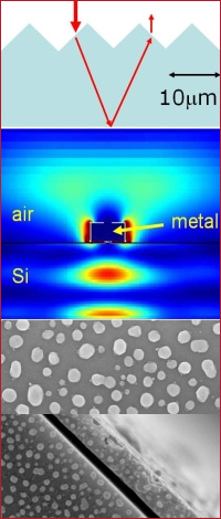
- Conventional solar cells are made from silicon wafers,
which are around 300 microns (1/3 of a millimetre) thick. The top surface of
these cells is covered with pyramids around 10 microns high. The pyramids
reduce the reflection from the top surface and trap the light inside the
solar cell (see figure A).
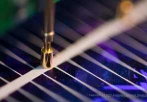
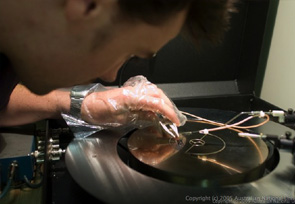
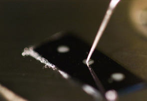
To reduce the cost of solar cells, thin film solar cells are being developed. These are only a few microns thick and have the potential to be much cheaper than conventional solar cells, because they use much less silicon. Pyramid textures can’t be applied to these cells, so new structures are needed. Unlike pyramid textures, which can be described with geometrical optics, we need wave optics to predict the behaviour of these new structures. In this project we are investigating how metal nanoparticles and nano-structured surfaces can be used to increase the amount of light absorbed in a solar cell, and hence increase the amount of electrical current generated. Figure B shows the intensity of the electromagnetic field around a nano-scale metal cylinder as it scatters light into a thin silicon solar cell. Because the metal particle is nanoscale and because of the high refractive index of the silicon, instead of reflecting the light the metal particle actually scatters the light into the silicon.
The metal particles are formed using a simple self-assembly process of evaporating a thin layer of metal and then annealing it at low temperature to form metal particles. Pictures C and D show the metal particles, only about 100nm across, taken with a scanning electron microscope.
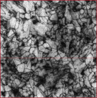
Silicon Materials
- Our research aims to understand the effects of defects and impurities in silicon solar cells, and to develop practical ways to reduce their impact, or remove them. This is particularly important when using low-cost silicon materials for solar cells, such as multicrystalline silicon wafers, or solar-grade silicon feedstocks, since these materials always contain significant quantities of unwanted impurities. The unwanted impurities of most interest are: dopants (such as B, P and Al), which are very difficult to remove during purification; metals (such as Fe, Cr, Ni etc), which can create strong recombination centres; and light elements (such as O, C and N), which may create defects that cause recombination or shunting. Crystal defects such as grain boundaries and dislocations also play an important role, and can interact with the impurities, for example, by acting as preferred sites for precipitation of metals.
In particular, our research focuses on the following topics:
- - The effect of transition metal impurities such as Fe, Cr, Ni and Cu on
solar cell performance.
- Development of sensitive, spatially resolved methods for detecting dopants and impurities in silicon wafers.
- The relative impact of defects and impurities in n- and p-type silicon. Many impurities are less problematic in n-type silicon, which has led to a renewed interest in this material for photovoltaics.
- Studying the relative recombination activity of dissolved or precipitated metals.
- Removal of metallic impurities such as Fe by heavily doped surface diffusions – a process known as ‘gettering’. We are especially interested in gettering of metals by boron diffusions, which are required for the development n-type multicrystalline silicon solar cells.
- Studying the impact of hydrogenation on dissolved and precipitated metals, and on crystal defects such as dislocations and grain boundaries.
- The use of Photoluminescence imaging and Photoluminescence Spectroscopy to study defects and impurities in silicon wafers.
- The study of intrinsic recombination processes in silicon - Auger and radiative recombination.
- Accurate measurement of the distributions and concentrations of impurities in solar-grade silicon feedstocks.
- The effects of dopant compensation (the simultaneous presence of p-type and n-type dopants) on carrier recombination and mobilities.
- Understanding the structure and evolution of the boron-oxygen defect, especially in relation to compensated silicon wafers.
We collaborate with a large number of institutes and companies in this area. Our major partners are: the Institute for Solar Energy Research Hameln (ISFH, Germany), the Energy Research Centre of the Netherlands (ECN), the Fraunhofer Institute for Solar Energy Systems (Fh-ISE), The University of New South Wales (UNSW), BT imaging, FerroAtlantica and CSG Solar.
Surface passivation
- The surfaces of solar cells are critical in
determining the overall performance of the devices. Typically, surfaces are
covered with one or more dielectric materials which serve to optimize both
the electronic and optical properties of the surfaces. They may also serve
other functions.
The interface properties depend on many factors, such as the deposition conditions and resulting detailed properties of the dielectric, the doping profile of the silicon in the near-surface region, the electric charge density in the dielectric, the surface crystal orientation and surface roughness, creating a large matrix of parameters for investigation.
Several dielectric materials are being studied in detail. These include silicon dioxide, silicon nitride, and titanium dioxide. Of particular interest are multilayer stacks in which two or more dielectrics are used to allow more flexibility in optimizing the electronic, optical and other required properties of the surface and interface regions.
We utilize a range of measurement techniques to obtain a good understanding of the material systems we are studying. These include charge carrier lifetime, capacitance-voltage, electron paramagnetic resonance, Kelvin probe, and ellipsometry measurements. 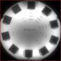
New Projects
- New projects include an ARC Linkage project with partners Spark Solar and Centrotherm to study aspects of surface passivation, and an ARC Linkage project with partners Spark Solar and BraggOne to study the application of spray-on films for the hydrogenation of the surface as well as the bulk of silicon wafers.
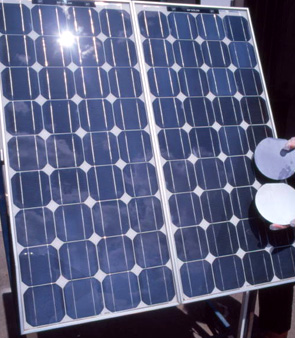
Silicon Solar Cells
- SLIVER solar cells are a new type of solar cell with the potential to revolutionise the global solar power industry. They were developed at the Centre for Sustainable Energy Systems with funding assistance from Origin Energy. SLIVER technology uses a revolutionary process to achieve high efficiencies while significantly reducing the amount of expensive silicon in solar cells. Solar modules made from SLIVERs can be lightweight, flexible and transparent and offer imaginative opportunities for building integration and other applications. By substantially improving the cost competitiveness of photovoltaics compared to electricity derived from fossil fuels, slivers have the potential to revolutionise the photovoltaics industry and simultaneously address the critical environmental issue of global warming.
SLIVER Technology Research
- A one-square-meter solar panel using SLIVER Cell
technology needs the equivalent of two silicon wafers to convert sunlight to
140 watts of power. By comparison, a conventional solar panel needs about 60
silicon wafers to achieve this performance. By dramatically reducing the
amount of expensive pure silicon, the largest cost in solar panels today,
this new technology represents a major advance in solar power technology.
The unique attributes of SLIVER Cell technology could open many new SLIVER
Cell applications, in addition to conventional rooftop and off-grid uses,
including:
- Transparent SLIVER Cell panes to replace building windows and cladding
- Flexible, roll-up solar panels
- High-voltage solar panels, and
- Solar powered aircraft, satellite and surveillance systems.
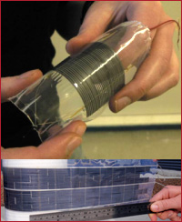
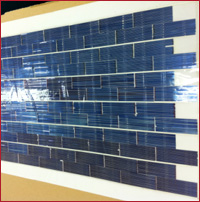
Flexible SLIVER modules
- Sliver cells have several properties that make them
ideally suited for use in flexible modules. Firstly, because they are
fabricated from mono-crystalline silicon they have high and stable
efficiencies. In addition, the elongate form factor of the cells means that
when connected in series, system voltage can be rapidly built, at a rate of
5 to 10 V/cm. Hence, battery voltage can be generated in a small area,
allowing cells to be incorporated into small portable electronic devices.
The dimensions of the cells mean they are naturally flexible, particularly
about their long axis, and do not require any post processing for them to be
incorporated into flexible modules. The cells are also lightweight, allowing
high power to weight ratios to be achieved. Also, because of the
non-destructive reverse breakdown properties of Sliver cells, bypass diodes
can be avoided, significantly reducing the complexity of the module design.
CSES is developing flexible photovoltaic modules based on SLIVER cells. The performance of these module is over 130 W/m2 with a power to weight ratio of greater than 150 W/kg, a radius of curvature of 5 cm or smaller, and operating temperatures between -40˚C and +65˚C. Modules can be either unifacial or bifacial depending on the desired application.
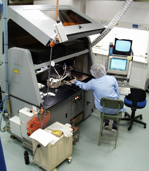
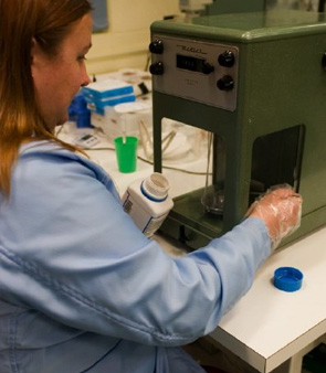
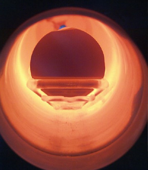
Image gallery
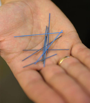
Sliver Cells (TM)
Linear trough concentrator
Semiconductors and devices
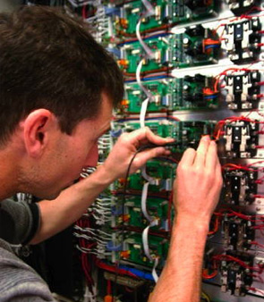
Photovoltaic Labs